
Razer Blade Gets Core i7-7700HQ, Adds 4K Touchscreen, 1 TB SSD Options
Razer this week introduced an upgraded version of its latest Blade laptop that is now powered by Intel’s quad-core Kaby Lake processor along with DDR4-2400 memory and has 4K display and 1 TB SSD options. The 14” gaming notebook uses the same 17.8 mm-thick chassis introduced last year and has the same I/O capabilities, but some minor differences in weight. Meanwhile, it is important to note that the entry-level Razer Blade now costs $100 less than it used to last year, but at the expense of a lower-resolution display.
The new Razer Blade is based on the Intel Core i7-7700HQ (4C/8T, 2.8/3.8 GHz, 6 MB, 45 W) processor as well as the HM175 PCH (so, the same motherboard as before). The new chip is powered by the Kaby Lake microarchitecture, has higher frequencies compared to its predecessor that was used in last year’s Blades (Core i7-6700HQ) and supports Speed Shift v2 technology as well as other improvements. Along with the Kaby Lake CPU, the new Blade also got 16 GB of faster DDR4-2400 memory (soldered to the mainboard). In addition to 256 GB and 512 GB M.2 (NVMe/PCIe) SSDs, Razer now also offers a 1 TB PCIe drive as an option. When it comes to graphics, the new Blade uses NVIDIA’s GeForce GTX 1060 with 6 GB of GDDR5 memory and an HDMI 2.0b output, just like the predecessor introduced last fall.
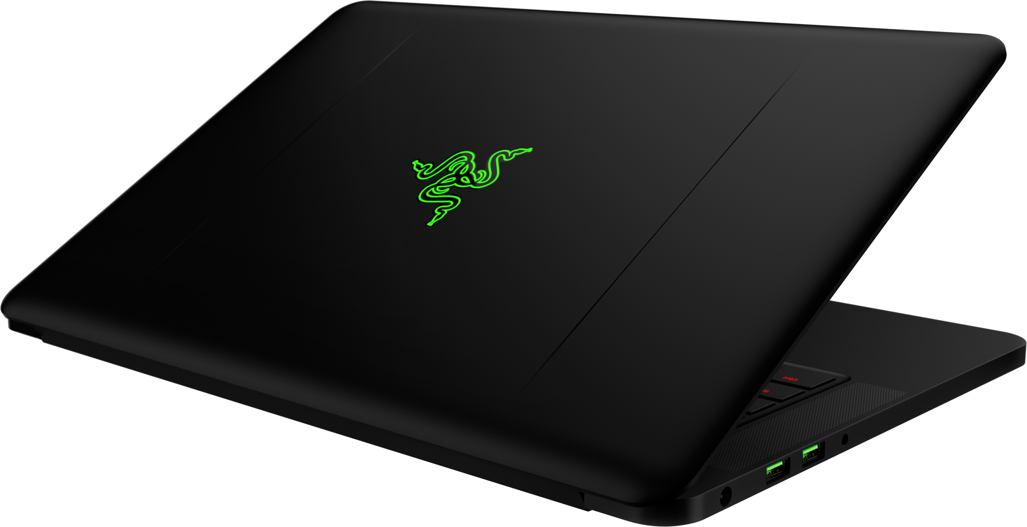
Apart from the CPU and DRAM upgrades, Razer changed display options for the latest breed of Blade laptops. Last year the company only offered its Blades with touch-enabled IGZO LCDs featuring 3200×1800 resolution, and a matte 1920×1080 on the entry level. This year the higher-end Blade machines will feature touch-enabled UHD displays (3840×2160). Usage of the lower-resolution panel allowed Razer to reduce the price of the entry-level Blade to $1899 (or by $100), but at present we do not know how much the 4K SKUs is going to cost. In any case, systems featuring FHD panels will be slightly lighter and will have a longer battery life than models with UHD monitors. We haven’t heard back from Razer on if the new UHD display continues to be a Sharp IGZO panel or not. Apart from displays, different Blade systems will look and feel exactly the same: both use a solid CNC-milled aluminum chassis with a matte black finish.
| Razer Blade Comparison | ||||||
| 2017 Razer Blade FHD | 2017 Razer Blade UHD | Late 2016 Razer Blade | ||||
| CPU | Intel Core i7-7700HQ 4C/8T 2.8 GHz/3.8 GHz 6 MB 45 W |
Intel Core i7-6700HQ 4C/8T 2.6/3.5 GHz 6 MB 47W |
||||
| GPU | NVIDIA GTX 1060 6 GB | |||||
| Memory | 16 GB DDR4-2400 | 16 GB DDR4-2133 | ||||
| Display | 1920×1080 matte | 3840×2160 touch | 3200×1800 IGZO touch | |||
| Storage | 256/512/1024 GB PCIe M.2 | 256/512 GB PCIe M.2 | ||||
| I/O | 3×USB 3.0 HDMI 2.0b Thunderbolt 3/USB-C |
|||||
| Wireless | Killer Wireless-AC 1535 | |||||
| Dimensions | 13.6″ × 9.3 ” × 0.70″ 345 mm × 235 mm × 17.8 mm |
|||||
| Weight | 1.86 kg 4.1 lbs |
1.95 kg 4.3 lbs |
1.93 kg 4.25 lbs |
|||
| Battery | 70 Wh | |||||
| Keyboard | Razer Chroma anti-ghosting | |||||
| Price | $1899 | unknown | $1999-$2199 | |||
As for the rest I/O capabilities, they remained very similar to those of the last year’s Razer Blade models (because the chassis and the motherboard are the same as those used on the late 2016 Blade): Rivet Networks’ Killer 1535 802.11 2×2 Wi-Fi + BT 4.1 controller, one Thunderbolt 3/USB 3.1 Type-C port, three USB 3.0 headers, an HDMI 2.0b output, a 2 MP webcam, built-in speakers and a microphone, a TRRS audio connector, a keyboard with RGB backlighting and so on. In a bid to appeal to those who care about security, there is a TPM 2.0 security chip installed.
The new Razer Blade notebooks with FHD screens are available now in North America and Europe starting from US$1,899/C$2,749/€2.149/£1.799. The laptops with 4K UHD panels will be available in Q2 and Razer does not have pricing available at the moment, but expect it to be similarly priced to the outgoing QHD+ model.

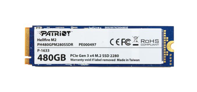
The Patriot Hellfire M.2 480GB
The Patriot Hellfire M.2 PCIe SSD is Patriot’s first NVMe SSD, and one of several similar products based on Phison’s E7 NVMe controller. As usual for Phison, the same drive is manufactured for many of their partners, who typically customize only the branding. Phison designs the controller, firmware, and PCB, but leaves the marketing up to their partners.
Phison’s PS5007-E7 controller is their first NVMe SSD controller, supporting a PCIe 3.0 x4 host interface and 8 channels for NAND access. The details we have on the E7 are a bit slim – some collection of ARM cores under the hood is a safe bet, but that’s it – however we do know that the E7 controller is manufactured on TSMC’s 28nm process and uses FCBGA packaging. Interestingly, it doesn’t use the kind of large heatspreader we’ve seen on competing controllers like Silicon Motion’s SM2260. Phison had the E7 platform hardware ready over a year ago, but retail releases were held back by the poor performance of early firmware. Patriot first began shipping the Hellfire last fall, but even after that much delay, they ended up issuing a firmware update shortly after launch.

Phison’s controllers are almost always paired with Toshiba’s NAND flash, and the Patriot Hellfire uses Toshiba’s 15nm MLC. Our review sample is the 480 GB version, the most common capacity for E7 SSD. Patriot also sells a 240 GB version, and some of their competitors offer the 120GB version as well.
| Patriot Hellfire Specifications Comparison | |||
| 240 GB | 480 GB | ||
| Form Factor | M.2 2280 | ||
| Controller | Phison PS5007-E7 | ||
| Interface | NVMe PCIe 3.0 x4 | ||
| DRAM | 256MB DDR3L | 512MB DDR3L | |
| NAND | Toshiba 15nm MLC | ||
| Sequential Read (CDM) | 2740 MB/s | 2550 MB/s | |
| Sequential Write | 1090 MB/s | 1260 MB/s | |
| 4KB Random Read (QD32) | 170k IOPS | 170k IOPS | |
| 4KB Random Write (QD32) | 185k IOPS | 210k IOPS | |
| Warranty | 3 years | ||
The Phison E7 controller was originally intended to be a high-end NVMe controller for client or enterprise use. By the time it was ready for the market, Samsung had raised the bar far too high for the E7 to still be considered high-end. But Phison E7-based SSDs like the Patriot Hellfire have been able to offer very attractive pricing and are usually the cheapest MLC-based NVMe SSDs available. Without the pitfalls of TLC-based SSDs like the Intel SSD 600p and the Samsung 960 EVO, the Patriot Hellfire and its relatives have been attractive entry-level PCIe SSD options.
Aside from other Phison E7 SSDs, the closest competition for the Patriot Hellfire is the Plextor M8Pe, based on the same Toshiba 15nm MLC NAND but using the Marvell 88SS1093 controller with Plextor’s own firmware. The Patriot Hellfire also has to justify its higher price relative to the Intel SSD 600p, the most affordable NVMe SSD, and against high-performing SATA SSDs like Samsung’s 850 EVO and 850 PRO.

SYBER VAPOR I REVIEW
PC games in the living room don’t get better than on CyberPower’s Syber Vapor
Highs
- Works as a viable console replacement out of the box
- Solid connectivity
- Performs well for its price
- Offers numerous customization options

Lows
- Initial cost might seem prohibitive to the console faithful
- Still stumbles in the most demanding games
With the Winter Steam Sale in full swing, there are a few questions that are fresh on the minds of PC gamers. What happened to the release of Steam OS? Why is Big Picture such an unstable mess? And when, if ever, will we see our first glimpse of Half Life 3?
While the first two are up to interpretation and the third will probably only be answered after the Second Coming, the missing answers haven’t been enough to stop the influx of party-ready PC/console hybrids that have shown up just in time for Santa to leave one under the tree.

Steam OS or no, the CyberPower’s Syber Vapor is well equipped to do the job it’s built to accomplish. With a 3.5GHz Core i3 processor, eight gigabytes of DDR3 RAM, a GTX 750Ti graphics card and one terabyte of available storage, the Vapor I is prepped for anything you have to throw its way and proves there’s might be something to PC/console hybrids after all.
Chunky, but loveable
The first thing we noticed about the Vapor I is that of the various Steam Machines we’ve reviewed over the past few weeks, this PC is considerably heavier than its cousins. At a shelf-crunching 36 pounds, the Vapor will be a hefty addition to anyone’s collection, though once it’s installed you won’t have any reason to move it again.
Measuring 13.8” long, 13.5” across, and 3.8” deep when laid on its side, the Vapor is a bit chunkier than most other entries in its class and noticeably larger than both the Xbox One and PS4. It’s still quite small for a gaming PC, though, and fits well enough in most home theaters.

Green LEDs line the Vapor’s exterior but fortunately aren’t bright enough be an annoyance, and while the case itself isn’t exactly sleek, the functionality this rig provides overrides our minor gripes about the system’s size and weight. It’s a simple, functional unit that looks slick without overdoing its style.
Ports! Ports! Get yer ports here
Connectivity is just the first of many areas the Vapor shines brighter than Rudolph’s nose. Let’s start with video. HDMI 1.4 and DVI-D are supported by the video card, which means the Vapor can handle resolutions up to 1440p.

Next to the video outputs we found four USB 2.0 ports, two USB 3.0, and an array of audio output and input options powered by a Realtek 7.1 channel surround sound chip integrated into the motherboard.
BY CHRIS STOBING

How do SSDs work?
To understand how and why SSDs are different from spinning discs, we need to talk a little bit about hard drives. A hard drive stores data on a series of spinning magnetic disks, called platters. There’s an actuator arm with read/write heads attached to it. This arm positions the read-write heads over the correct area of the drive to read or write information.
Because the drive heads must align over an area of the disk in order to read or write data (and the disk is constantly spinning), there’s a non-zero wait time before data can be accessed. The drive may need to read from multiple locations in order to launch a program or load a file, which means it may have to wait for the platters to spin into the proper position multiple times before it can complete the command. If a drive is asleep or in a low-power state, it can take several seconds more for the disk to spin up to full power and begin operating.
From the very beginning, it was clear that hard drives couldn’t possibly match the speeds at which CPUs could operate. Latency in HDDs is measured in milliseconds, compared with nanoseconds for your typical CPU. One millisecond is 1,000,000 nanoseconds, and it typically takes a hard drive 10-15 milliseconds to find data on the drive and begin reading it. The hard drive industry introduced smaller platters, on-disk memory caches, and faster spindle speeds to counteract this trend, but there’s only so fast that drives can spin. Western Digital’s 10,000 RPM VelociRaptor family is the fastest set of drives ever built for the consumer market, while some enterprise drives spun up to 15,000 RPM. The problem is, even the fastest spinning drive with the largest caches and smallest platters are still achingly slow as far as your CPU is concerned.
How SSDs are different
“If I had asked people what they wanted, they would have said faster horses.” — Henry Ford
Solid-state drives are called that specifically because they don’t rely on moving parts or spinning disks. Instead, data is saved to a pool of NAND flash. NAND itself is made up of what are called floating gate transistors. Unlike the transistor designs used in DRAM, which must be refreshed multiple times per second, NAND flash is designed to retain its charge state even when not powered up. This makes NAND a type of non-volatile memory.
The diagram above shows a simple flash cell design. Electrons are stored in the floating gate, which then reads as charged “0” or not-charged “1.” Yes, in NAND flash, a 0 means that data is stored in a cell — it’s the opposite of how we typically think of a zero or one. NAND flash is organized in a grid. The entire grid layout is referred to as a block, while the individual rows that make up the grid are called a page. Common page sizes are 2K, 4K, 8K, or 16K, with 128 to 256 pages per block. Block size therefore typically varies between 256KB and 4MB.
One advantage of this system should be immediately obvious. Because SSDs have no moving parts, they can operate at speeds far above those of a typical HDD. The following chart shows the access latency for typical storage mediums given in microseconds.

NAND is nowhere near as fast as main memory, but it’s multiple orders of magnitude faster than a hard drive. While write latencies are significantly slower for NAND flash than read latencies, they still outstrip traditional spinning media.
There are two things to notice in the above chart. First, note how adding more bits per cell of NAND has a significant impact on the memory’s performance. It’s worse for writes as opposed to reads — typical triple-level-cell (TLC) latency is 4x worse compared with single-level cell (SLC) NAND for reads, but 6x worse for writes. Erase latencies are also significantly impacted. The impact isn’t proportional, either — TLC NAND is nearly twice as slow as MLC NAND, despite holding just 50% more data (three bits per cell, instead of two).

The reason TLC NAND is slower than MLC or SLC has to do with how data moves in and out of the NAND cell. With SLC NAND, the controller only needs to know if the bit is a 0 or a 1. With MLC NAND, the cell may have four values — 00, 01, 10, or 11. With TLC NAND, the cell can have eight values. Reading the proper value out of the cell requires that the memory controller use a very precise voltage to ascertain whether any particular cell is charged or not.
Reads, writes, and erasure
One of the functional limitations of SSDs is that while they can read and write data very quickly to an empty drive, overwriting data is much slower. This is because while SSDs read data at the page level (meaning from individual rows within the NAND memory grid) and can write at the page level, assuming that surrounding cells are empty, they can only erase data at the block level. This is because the act of erasing NAND flash requires a high amount of voltage. While you can theoretically erase NAND at the page level, the amount of voltage required stresses the individual cells around the cells that are being re-written. Erasing data at the block level helps mitigate this problem.
The only way for an SSD to update an existing page is to copy the contents of the entire block into memory, erase the block, and then write the contents of the old block + the updated page. If the drive is full and there are no empty pages available, the SSD must first scan for blocks that are marked for deletion but that haven’t been deleted yet, erase them, and then write the data to the now-erased page. This is why SSDs can become slower as they age — a mostly-empty drive is full of blocks that can be written immediately, a mostly-full drive is more likely to be forced through the entire program/erase sequence.
If you’ve used SSDs, you’ve likely heard of something called “garbage collection.” Garbage collection is a background process that allows a drive to mitigate the performance impact of the program/erase cycle by performing certain tasks in the background. The following image steps through the garbage collection process.

Note that in this example, the drive has taken advantage of the fact that it can write very quickly to empty pages by writing new values for the first four blocks (A’-D’). It’s also written two new blocks, E and H. Blocks A-D are now marked as stale, meaning they contain information that the drive has marked as out-of-date. During an idle period, the SSD will move the fresh pages over to a new block, erase the old block, and mark it as free space. This means that the next time the SSD needs to perform a write, it can write directly to the now-empty Block X, rather than performing the program/erase cycle.
The next concept I want to discuss is TRIM. When you delete a file from Windows on a typical hard drive, the file isn’t deleted immediately. Instead, the operating system tells the hard drive that it can overwrite the physical area of the disk where that data was stored the next time it needs to perform a write. This is why it’s possible to undelete files (and why deleting files in Windows doesn’t typically clear much physical disk space until you empty the recycling bin). With a traditional HDD, the OS doesn’t need to pay attention to where data is being written or what the relative state of the blocks or pages is. With an SSD, this matters.
The TRIM command allows the operating system to tell the SSD that it can skip rewriting certain data the next time it performs a block erase. This lowers the total amount of data that the drive writes and increases SSD longevity. Both reads and writes damage NAND flash, but writes do far more damage than reads. Fortunately, block-level longevity has not proven to be an issue in modern NAND flash. More data on SSD longevity, courtesy of the Tech Report, can be found here.
The last two concepts we want to talk about are wear leveling and write amplification. Because SSDs write data to pages but erase data in blocks, the amount of data being written to the drive is always larger than the actual update. If you make a change to a 4KB file, for example, the entire block that 4K file sits within must be updated and rewritten. Depending on the number of pages per block and the size of the pages, you might end up writing 4MB worth of data to update a 4KB file. Garbage collection reduces the impact of write amplification, as does the TRIM command. Keeping a significant chunk of the drive free and/or manufacturer overprovisioning can also reduce the impact of write amplification.
Wear leveling refers to the practice of ensuring that certain NAND blocks aren’t written and erased more often than others. While wear leveling increases a drive’s life expectancy and endurance by writing to the NAND equally, it can actually increase write amplification. In other to distribute writes evenly across the disk, it’s sometimes necessary to program and erase blocks even though their contents haven’t actually changed. A good wear leveling algorithm seeks to balance these impacts.
The SSD controller
It should be obvious by now that SSDs require much more sophisticated control mechanisms than hard drives do. That’s not to diss magnetic media — I actually think HDDs deserve more respect than they are given. The mechanical challenges involved in balancing multiple read-write heads nanometers above platters that spin at 5,400 to 10,000 RPM are nothing to sneeze at. The fact that HDDs perform this challenge while pioneering new methods of recording to magnetic media and eventually wind up selling drives at 3-5 cents per gigabyte is simply incredible.

SSD controllers, however, are in a class by themselves. They often have a DDR3 memory pool to help with managing the NAND itself. Many drives also incorporate single-level cell caches that act as buffers, increasing drive performance by dedicating fast NAND to read/write cycles. Because the NAND flash in an SSD is typically connected to the controller through a series of parallel memory channels, you can think of the drive controller as performing some of the same load balancing work as a high-end storage array — SSDs don’t deploy RAID internally, but wear leveling, garbage collection, and SLC cache management all have parallels in the big iron world.
Some drives also use data compression algorithms to reduce total number of writes and improve the drive’s lifespan. The SSD controller handles error correction, and the algorithms that control for single-bit errors have become increasingly complex as time has passed.
Unfortunately, we can’t go into too much detail on SSD controllers because companies lock down their various secret sauces. Much of NAND flash’s performance is determined by the underlying controller, and companies aren’t willing to lift the lid too far on how they do what they do, lest they hand a competitor an advantage.
The road ahead
NAND flash offers an enormous improvement over hard drives, but it isn’t without its own drawbacks and challenges. Drive capacities and price-per-gigabyte are expected to continue to rise and fall respectively, but there’s little chance that SSDs will catch hard drives in price-per-gigabyte. Shrinking process nodes are a significant challenge for NAND flash — while most hardware improves as the node shrinks, NAND becomes more fragile. Data retention times and write performance are intrinsically lower for 20nm NAND than 40nm NAND, even if data density and total capacity are vastly improved.
Thus far, SSD manufacturers have delivered better performance by offering faster data standards, more bandwidth, and more channels per controller — plus the use of SLC caches we mentioned earlier. Nonetheless, in the long run, it’s assumed that NAND will be replaced by something else.
What that something else will look like is still open for debate. Both magnetic RAM and phase change memory have presented themselves as candidates, though both technologies are still in early stages and must overcome significant challenges to actually compete as a replacement to NAND. Whether consumers would notice the difference is an open question. If you’ve upgraded from NAND to an SSD and then upgraded to a faster SSD, you’re likely aware that the gap between HDDs and SSDs is much larger than the SSD – SSD gap, even when upgrading from a relatively modest drive. Improving access times from milliseconds to microseconds matters a great deal, but improving them from microseconds to nanoseconds might fall below what humans can realistically perceive in most cases.
Intel’s 3D XPoint (marketed as Intel Optane) has emerged as one potential challenger to NAND flash, and the only current alternative technology in mainstream production (other alternatives, like phase-change memory or magnetoresistive RAM. Intel has played its cards close to the vest with Optane and hasn’t revealed many of its underlying technologies, but we’ve recently seen some updated information on the company’s upcoming Optane SSDs.

Optane SSDs are expected to offer similar sequential performance to current NAND flash drives, but with vastly better performance at low drive queues. Drive latency is also roughly half of NAND flash (10 microseconds, versus 20) and vastly higher endurance (30 full drive-writes per day, compared with 10 full drive writes per day for a high-end Intel SSD). For now, Optane is still too new and expensive to match NAND flash, which benefits from substantial economies of scale, but this could change in the future. The first Optane SSDs will debut this year as add-ons for Kaby Lake and its X270 chipset. NAND will stay king of the hill for at least the next 4-5 years. But past that point we could see Optane starting to replace it in volume, depending on how Intel and Micron scale the technology and how well 3D NAND flash continues to expand its cell layers (64-layer NAND will ship in 2017 from multiple players), with roadmaps for 96 and even 128 layers on the horizon.
By Joel Hruska

Intel’s 8th gen chips will still use 14nm, will arrive earlier than expected
Last year, Intel announced that it would abandon the Tick-Tock model that had served it for nearly a decade and switch to something called PAO — Process, Architecture, Optimization. The point of switching from a two-step process to a three-step system was to give Intel extra time to roll out its next-generation process nodes, while simultaneously affording more opportunity to eke maximum gains out of each current node. Now, new information suggests Intel may have a product plan that tears up PAO (or at least complicates it) going forward.
Analyst Ashraf Eassa claims to have confirmed with Intel that upcoming 8th generation Core processors will use an updated/enhanced variant of 14nm technology yet again — call it 14nm++. Intel was able to squeeze some gains out of Kaby Lake in this fashion compared with Skylake, but they weren’t huge leaps.

A slide showed by Intel at a recent speech on the future of its data center business confirms this by stating “Data center first to next process node,” Anandtech notes. It also makes the point that enterprise and government spending are only worth a 2% increase in CAGR (Compound Annual Growth Rate) while the cloud services business is expected to grow by 15% from 2017-2021.
Still, at first glance, this may seem a foolish strategy. After all, AMD’s Ryzen will debut in the imminent future, and one might reasonably conclude that Intel’s best leap forward is with a strong 10nm chip rather than a third iteration on 14nm. But this misses a larger issue — one we’ve discussed multiple times over the past few years. As node shrinks become more difficult and the advantages of any given node shrink are less and less potent, it can take longer for a company to deliver meaningful advantages. Intel is still pursuing full node shrinks, unlike its competitors at GlobalFoundries, Samsung, and TSMC. These firms won’t offer equivalent gate lengths or feature sizes to Intel until they deploy their 10nm nodes and aren’t expected to match Intel’s 10nm until they hit 7nm. This is why Intel can still plausibly claim to be ahead on process technology, despite using a higher number to describe it.

When Intel debuted 14nm, it pushed that technology into ultra-mobile parts first, where the reduction in power consumption and improvement of low-power clock speeds was seen as critical to the company’s ability to compete with ARM. As we’ve recently discussed, the improvements to Intel’s low-power CPUs have been considerably larger than the boosts to desktop performance in an equivalent period of time. AMD, prior to Ryzen, has been stuck in a similar scenario.
We may be arriving at a point where it makes more sense to keep older nodes around and to improve process nodes and architecture over several generations than it does to aggressively transition to each new node. Earlier this year, Mark Papermaster of AMD made comments to suggest that AMD would stick to 14nm for multiple product generations. It’s not clear how this will play out or how aggressively the smaller CPU manufacturer will use the strategy. But we could be seeing a similar play from Intel, which has already deployed 14nm across three families of processors (Broadwell, Skylake, Kaby Lake) and may be prepping desktop Cannon Lake chips for a fourth. Other foundry manufacturers have begun referring to certain nodes as “long-lived” (28nm, 14/16nm, and possibly 7nm) while others (20nm, 10nm) are being described as short-term nodes. This differentiation didn’t used to exist in semiconductor technology and it indirectly speaks to what Intel may be driving at: Some nodes are better than others for certain types of semiconductors.
8th-gen chips on 14nm are now expected in the second half of 2017 rather than the first half of 2018 as had previously been reported. This could mean Intel wants to push new hardware to compete with Ryzen sooner than later.
Intel might defend PAO as a process with an undisclosed number of steps in the “Optimization” portion, rather than a discrete series of changes that was meant to apply to three, and only three, groups of processors. This interpretation is undermined by how Intel raised precisely zero objections last year when the world+dog described PAO as a three-step process compared with the two-stop pendulum model of tick-tock. We may see multiple process nodes gathered together under the 8th Generation Core banner, with ultra-low-power mobile and data center chips moving to 10nm first, while desktop and high-power laptop processors following at a later date.
By Joel Hruska

 Mood
Mood
- 27 days left until Tomorrowland Belgium.
- 28 days left until Tomorrowland Belgium.
- 29 days left until Tomorrowland Belgium.
- 30 days left until Tomorrowland Belgium.
- 31 days left until Tomorrowland Belgium.
- 32 days left until Tomorrowland Belgium.
- 33 days left until Tomorrowland Belgium.
- 34 days left until Tomorrowland Belgium.
- 12 juni 2026
- 36 days left until Tomorrowland Belgium.
- Tomorrowland - One World Radio
- 37 days left until Tomorrowland Belgium.
- 38 days left until Tomorrowland Belgium.
- 39 days left until Tomorrowland Belgium.
- 7 juni 2026